How to select TVS diodes (ESD protection diodes) based on the voltage level of the signal lines that need to be protected?
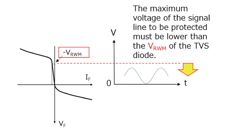
For example, given below is the diagram contained in the datasheet of a unidirectional TVS diode (definition of electrical characteristics). While TVS diodes come in many voltage and current specifications, attention should be paid to the operating peak reverse voltage (VRWM) here.
VRWM is a threshold below which the TVS diode remains off when Ta=25°C. Therefore, TVS diodes with VRWM higher than the maximum voltage of the signal line to be protected must be selected.
However, if ESD occurs, TVS diodes with too high VRWM (i.e. high clamping voltage) will cause more energy to flow into the protected device. Please select the best TVS diode according to the design specifications.

What should you pay attention to when TVS diodes (ESD protection diodes) are not working properly?
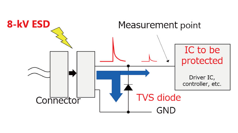
Even if there is an ESD protection device, if the IC to be protected is still damaged by static electricity, it indicates that the ESD protection performance for this IC is insufficient. Special care should be taken when the ESD immunity of the IC to be protected is low.
The graph below compares the first peak voltage at the input of the IC after replacing two different TVS diodes. Although functionally similar, these TVS diodes exhibit different clamping voltages. (Product A: Typical value is 9.6V at 4A; Product B: Typical value is 13V at 4A). This figure shows that product A has stronger protection against ESD pulses. Note that even similar TVS diodes can have very different ESD protection performance.

Circuit board design considerations for TVS diodes (ESD protection diodes)
Even TVS diodes with high ESD protection performance may not provide adequate ESD protection if the circuit board design is inadequate. In particular, circuit board design will affect the transient high-frequency pulses generated after ESD enters.
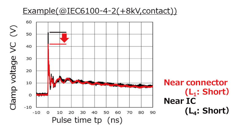
The figure below compares clamping voltage waveforms depending on the distance between the TVS diode and the connector and the ESD entry point. As can be seen from the figure, when the TVS diode is positioned close to the connector (i.e., away from the protected IC), the first peak voltage (i.e., the voltage after ESD entry) is almost 10V lower than when the TVS diode is positioned close to the IC.

When designing a circuit board, pay attention to the following points:
1. The TVS diode should be located as close to the connector as possible (to minimize the length of the L1 trace).
2. Reduce the length of L2 and L3 behind the TVS diode.
3. Do not use vias (through holes) in the L2 and L3 traces.
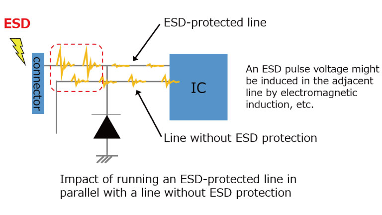
4. Do not run ESD-protected lines connected to ESD entry points parallel to non-ESD-protected lines. These lines should not be parallel, especially the lines from the ESD entry point to the TVS diode.

About Semiware
Semiware has a comprehensive product lineup of circuit protection device products. The company leverages its technology in the semiconductor field and application background in end products to serve customers in the electronics, automotive and industrial markets. For more information, please visit semiware official website: https://semiware.com
Tel: +86-21-3463-7654;
Toll-free technical support hotline: +86-400-021-5756
Comments (0)